Using Design Of Experiments To Optimize Wire Bond Processes
September 10, 2016
Minnowbrook Microelectronics Conference
September 14, 2016
IMAPS NE Symposium’s Technical Chairs Welcome Letter
We’d like to welcome everyone to the 41st Annual New England IMAPS Symposium! We have compiled an excellent selection of technical presentations representing a diversity of interests in the microelectronics packaging field. Thanks to the Session Chairs and Technical Committee for all of their time and effort. As an Attendee, it’s your job to reach out and meet someone new, learn something new and challenge the speakers on their technical content. The open, back-and-forth dialog on complex technical issues benefits everyone. So put away the cell phones and do some real time Face-booking. Here are the technical highlights, please take full advantage.
Counterfeit
Prevention & Mitigation Strategies: Counterfeits today are pervasive, impacting today’s distributed global supply chain. Presentations in this session include specialized taggant technologies & the DLA mandate, issues pertaining to RoHS component, packaging & processor technologies, analysis /assessment of QC non-conformance issues, which appear similar to counterfeiting techniques and the proper implementation /qualification of PEMs for use in aerospace and DOD applications.
RF and Microwave
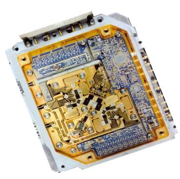
Innovations and Emerging Technologies: This session is about the innovations and emerging technologies that are driving RF and microwave packaging. Discussion begins with the topic of integration in RF ICs followed by a presentation from Cree on high power packaging of GaN chips. The next two presentations address package design using HTCC and tungsten-copper substrates. Hittite and NXP bring us up-to-speed on technical issues at the device level. Finally, just after lunch we have two excellent papers discussing non-hermetic packaging and encapsulation of RF microwave devices.
Bumped Die Attach
Covers a lot of ground with papers from numerous sectors of this industry. Engent will update us with the latest on copper wire bonded interconnections followed by DuPont with a talk on BGA attach on Green Tape and then a presentation on thermosonic flip chip methods on Cu. DFR will discuss reliability issues in flip chip design and then a talk on solid state micro-batteries.
NANO and MEMS
Technologies on the Move: MEMS applications are blossoming – from multiple airbag sensors, flow control and stability control in automobiles to gyroscopes, microphones and tuners in handheld devices. New sensor systems – optical, bio and other – are now gaining traction. Nanomaterial applications are starting to blossom in the electronics industry, from stencil coatings to fillers in underfills, surface finishes, and tin whisker mitigation coatings – the list is growing fast. This session represents the best of both worlds!
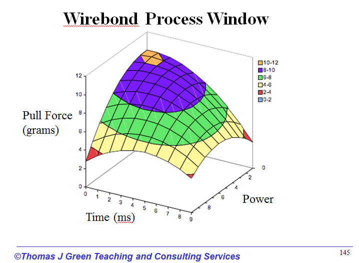
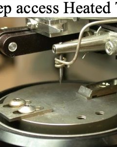
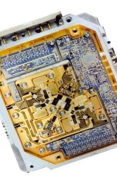
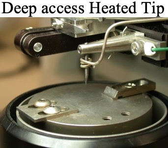
Wire Bonding & Advanced Interconnections (Cu)
The entire spectrum of wire bonding technologies is explored. Sensata Technologies presents on how to avoid heel cracks during ultrasonic wire bonding. The IPC Committee represented by Uyemura, will then present their latest wire bondable nickel plating proposal with Al and Cu wire bonding to ENIG & ENEPIG. We’ll then hear about a robust gold stitch-to-substrate wire bond attach and Hesse Mechatronics will update us on heavy copper wire bonding in power electronics.
Novel Technologies
This session includes results on a study of newly developed nano silver pastes with metallo-organic technology and a talk from Brookhaven National Laboratories on a particle tracking device. A presentation from the Boston Retinal Implant Project will be a nice complement to our Luncheon speaker.
Technologies and Methods for 2.5/3D Packaging
This session covers the latest advancements in pre-applied material for 2.5/3D utilizing interposer technology and glass interposer substrates, then a discussion on molded and measured lithographic process capabilities to achieve critical dimensions. Also, reviews of advances in die attach film, temporary wafer protection, and enabling technology for 3D integration.